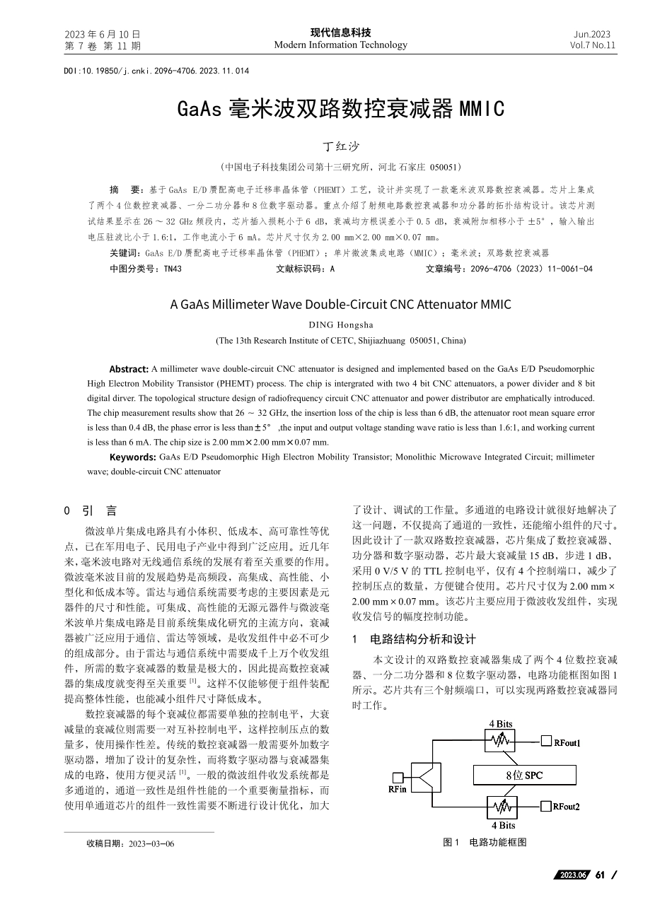
2023年6月10日第7卷第11期现代信息科技ModernInformationTechnologyJun.2023Vol.7No.1161612023.062023.06收稿日期:2023-03-06GaAs毫米波双路数控衰减器MMIC丁红沙(中国电子科技集团公司第十三研究所,河北石家庄050051)摘要:基于GaAsE/D赝配高电子迁移率晶体管(PHEMT)工艺,设计并实现了一款毫米波双路数控衰减器。芯片上集成了两个4位数控衰减器、一分二功分器和8位数字驱动器。重点介绍了射频电路数控衰减器和功分器的拓扑结构设计。该芯片测试结果显示在26~32GHz频段内,芯片插入损耗小于6dB,衰减均方根误差小于0.5dB,衰减附加相移小于±5°,输入输出电压驻波比小于1.6:1,工作电流小于6mA。芯片尺寸仅为2.00mm×2.00mm×0.07mm。关键词:GaAsE/D赝配高电子迁移率晶体管(PHEMT);单片微波集成电路(MMIC);毫米波;双路数控衰减器中图分类号:TN43文献标识码:A文章编号:2096-4706(2023)11-0061-04AGaAsMillimeterWaveDouble-CircuitCNCAttenuatorMMICDINGHongsha(The13thResearchInstituteofCETC,Shijiazhuang050051,China)Abstract:Amillimeterwavedouble-circuitCNCattenuatorisdesignedandimplementedbasedontheGaAsE/DPseudomorphicHighElectronMobilityTransistor(PHEMT)process.Thechipisintergratedwithtwo4bitCNCattenuators,apowerdividerand8bitdigitaldirver.ThetopologicalstructuredesignofradiofrequencycircuitCNCattenuatorandpowerdistributorareemphaticallyintroduced.Thechipmeasurementresultsshowthat26~32GHz,theinsertionlossofthechipislessthan6dB,theattenuatorrootmeansquareerrorislessthan0.4dB,thephaseerrorislessthan±5°,theinputandoutputvoltagestandingwaveratioislessthan1.6:1,andworkingcurrentislessthan6mA.Thechipsizeis2.00mm×2.00mm×0.07mm.Keywords:GaAsE/DPseudomorphicHighElectronMobilityTransistor;MonolithicMicrowaveIntegratedCircuit;millimeterwave;double-circuitCNCattenuator0引言微波单片集成电路具有小体积、低成本、高可靠性等优点,已在军用电子、民用电子产业中得到广泛应用。近几年来,毫米波电路对无线通信系统的发展有着至关重要的作用。微波毫米波目前的发展趋势是高频段,高集成、高性能、小型化和低成本等。雷达与通信系统需要考虑的主要因素是元器件的尺寸和性能。可集成、高性能的无源元器件与微波毫米波单片集成电路是目前系统集成化研究的主...