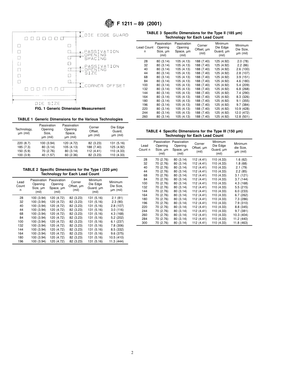
分享
ASTM_F_1211_-_89_2001.pdf
下载文档

ID:188138

大小:32.91KB

页数:3页

格式:PDF

时间:2023-03-04

收藏 分享赚钱
温馨提示:
1. 部分包含数学公式或PPT动画的文件,查看预览时可能会显示错乱或异常,文件下载后无此问题,请放心下载。
2. 本文档由用户上传,版权归属用户,汇文网负责整理代发布。如果您对本文档版权有争议请及时联系客服。
3. 下载前请仔细阅读文档内容,确认文档内容符合您的需求后进行下载,若出现内容与标题不符可向本站投诉处理。
4. 下载文档时可能由于网络波动等原因无法下载或下载错误,付费完成后未能成功下载的用户请联系客服处理。
网站客服:3074922707
TM_F_1211_ _89_2001
Designation:F 1211 89(Reapproved 2001)Standard Specification forSemiconductor Device Passivation Opening Layouts1This standard is issued under the fixed designation F 1211;the number immediately following the designation indicates the year oforiginal adoption or,in the case of revision,the year of last revision.A number in parentheses indicates the year of last reapproval.Asuperscript epsilon(e)indicates an editorial change since the last revision or reapproval.1.Scope1.1 This specification covers standard semiconductor devicepassivation opening layouts for various tape automated bond-ing interconnection technologies.1.2 This specification established the nominal passivationopening dimensions,nominal passivation,opening spacing,nominal corner passivation opening offset,minimum scribeguard and minimum die size for the most common input/outputcounts within each technology.1.3 This specification is extendable to other interconnectiontechnologies if the passivation opening and spacing are ad-justed in such a way that the progression is not modified.1.4 The values stated in SI units are to be regarded as thestandard.The values given in parentheses are for informationonly.2.Terminology2.1 Definitions:2.1.1 corner offsetThe orthogonal distance between thecorner passivation opening on adjacent sides of the die wherea corner passivation opening is indentified as the end passiva-tion opening on a die side.2.1.2 lead countThe number of passivation openingsavailable on a fully populated die layout.2.1.3 minimum die edge guardThe minimum distancebetween the die edge and the passivation opening nearest to thedie edge herein used to establish the minimum die size.2.1.4 minimum die sizeThe minimum die size is calcu-lated by the following equation:minimum die size 5 lead count/4!p.o.size 1 p.o.space!2 p.o.space 1 2 corner offset 1 p.o.size1 die edge guard!2.1.5 passivation openingThe unpassivated area withinthe device metal bonding pad area.2.1.6 passivation opening sizeThe minimum othagonaldimensions of the passivation opening for the particulartechnology herein used as the nominal passivation openingsize.2.1.7 passivation opening spaceThe minimum space be-tween adjacent passivation openings for the particular technol-ogy herein used as the nominal passivation opening spacing.2.1.8 progressionThe dimension as measured from areference point on one passivation opening to the samereference point on the adjacent passivation opening.2.1.9 technologyThe minimum passivation opening pro-gression allowable for a specific interconnection method.3.Classification3.1 The passivation opening layouts are separated into fourtechnology types where:Type I=220 m technology(220 m=8.7 mils)Type II=185 m technology(185 m=7.3 mils)Type III=150 m technology(150 m=5.9 mils)Type IV=100 m technology(100 m=3.9 mils)4.Dimensions,Mass,and Permissible Variations4.1 The primary unit of measure is micrometres(m)(1micrometre=1 micron)and the secondary unit of measure ismils(1/1000 of an in.),where 1 mil(0.001 in.)=25.4 m.4.2 Fig.1 shows the generic dimension measurement foreach defined dimension.4.3 The lead count independent dimensions are summarizedin Table 1 for all technologies.4.4 The specific standard layouts are listed in Tables 2-5 forType I,Type II,Type III and Type IV technologies respectively.4.5 ProgressionAny variations must be noncumulative.4.6 Lead CountAll passivation openings as specified inthis specification must be included in the design whether theyare or are not connected internally.5.Keywords5.1 opening layouts;passivation;semiconductor devices1This specification is under the jurisdiction of ASTM Committee F01 onElectronics and is the direct responsibility of Subcommittee F01.07 on WireBonding,Flip Chip,and Tape Automated Bonding.Current edition approved Feb.24,1989.Published April 1989.1Copyright ASTM International,100 Barr Harbor Drive,PO Box C700,West Conshohocken,PA 19428-2959,United States.FIG.1 Generic Dimension MeasurementTABLE 1 Generic Dimensions for the Various TechnologiesTechnology,m(mil)PassivationOpeningSize,m(mil)PassivationOpeningSpace,m(mil)CornerOffset,m(mil)Die EdgeGuard,m(mil)220(8.7)100(3.94)120(4.72)82(3.23)131(5.16)185(7.3)80(3.14)105(4.13)188(7.40)125(4.92)150(5.9)70(2.76)80(3.14)112(4.41)110(4.33)100(3.9)40(1.57)60(2.36)82(3.23)110(4.33)TABLE 2 Specific Dimensions for the Type I(220 m)Technology for Each Lead CountLeadCountnPassivationOpeningSize,m(mil)PassivationOpeningSpace,m(mil)CornerOffset,m(mil)MinimumDie EdgeGuard,m(mil)MinimumDie Size,m(mil)28100(3.94)120(4.72)82(3.23)131(5.16)2.1(81)32100(3.94)120(4.72)82(3.23)131(5.16)2.3(90)40100(3.94)120(4.72)82(3.23)131(5.16)2.8(107)44100(3.94)120(4.72)82(3.23)131(5.16)3.0(116)68100(3.94)120(4.72)82(3.23)131(5.16)4.3(168)84100(3.94)120(4.72)82(3.23)131(5.16)5.2(202)100100(3.94)120(4.72)82(3.23)131(5.16)6.1(237)132100(3.94)120(4.72)82(3.23)131(5.16)7.8(306)144100(3.94)120(4.72)82(3.23)131(5.16)8.5(332)164100(3.94)120(4.72)82(3.23)131(5.16)9.6(375)180100(3.94)120(4.

此文档下载收益归作者所有

下载文档
你可能关注的文档
收起
展开